
ACL Digital
June 13, 2025
5 Minutes read
EDA Tools and Cloud Integration: A New Frontier in Silicon Engineering
The increasing complexity of modern semiconductor designs, driven by the demand for smaller nodes, higher transistor densities, and advanced process technologies, has pushed traditional on-premises Electronic Design Automation (EDA) workflows to their limits. Conventional EDA environments, constrained by fixed compute resources, struggle to handle the exponential rise in verification cycles, design iterations, and deep learning-driven optimization techniques. As a result, silicon engineering is undergoing a paradigm shift with cloud-integrated EDA solutions. Cloud-based EDA leverages high-performance, scalable computing, allowing real-time parallel processing for synthesis, place-and-route, and verification workloads. By eliminating the bottlenecks of hardware limitations, accelerating design convergence, and enabling seamless collaboration across global design teams, cloud-powered EDA is not just an enhancement but is redefining the future of semiconductor innovation.
Cloud-Optimized EDA Architectures: Beyond On-Prem Limitations
Cloud-integrated EDA solutions are not merely an extension of traditional design environments—they represent a fundamental shift in how semiconductor workflows are executed. By leveraging distributed computing, real-time parallelism, and AI-driven automation, cloud-native EDA architectures address the limitations of on-premises systems and unlock new efficiencies in chip design.
- Scalable Compute Clusters: Unlike fixed on-premise infrastructures, cloud-based EDA platforms dynamically allocate compute resources based on workload demands. This scalability enables faster execution of complex tasks such as multi-dimensional design exploration, advanced timing signoff, and power integrity analysis, significantly reducing turnaround time.
- Lift-and-Shift vs. Cloud-Native EDA: Migrating traditional EDA tools to virtualized cloud environments offers some flexibility, but it does not fully harness cloud capabilities. Cloud-native EDA solutions like Cadence Cloud, Synopsys Cloud, and Siemens EDA on AWS are designed to optimize distributed processing, enable elastic scaling, and integrate seamlessly with AI-driven design optimizations. These solutions eliminate the inefficiencies of legacy workflows and provide real-time collaboration across geographically dispersed design teams.
- Specialized Hardware for Acceleration: Cloud-based silicon design benefits from hardware accelerators such as FPGA-based cloud instances, which enhance computational workloads for RTL simulation, synthesis, and hardware emulation. These accelerators improve performance in verification, functional safety analysis, and AI-powered optimization, offering a cost-effective alternative to dedicated on-premise infrastructure.
AI-Enhanced EDA in the Cloud: Automating and Optimizing Chip Design
Integrating AI into cloud-based EDA workflows is transforming semiconductor design, enabling intelligent automation, faster optimizations, and superior Power, Performance, and Area (PPA) outcomes. AI-powered algorithms leverage vast computational resources in the cloud to analyze complex design spaces, predict optimal configurations, and accelerate verification cycles.
- AI-Driven Design Space Exploration (DSE): Cloud-based AI models analyze millions of design parameters in real-time, optimizing PPA trade-offs with unparalleled efficiency. By leveraging machine learning algorithms, engineers can identify the best configurations for power efficiency, timing closure, and area reduction without exhaustive manual iterations.
- AI-Based Layout Synthesis and Physical Verification: AI accelerates place-and-route optimization and physical verification by learning from past design data and predicting optimal layouts. Cloud-integrated AI models enhance Design Rule Checking (DRC), Layout vs. Schematic (LVS) validation, and parasitic extraction, reducing error rates and improving design accuracy.
- Cloud-Powered Reinforcement Learning for Circuit Design: AI-driven reinforcement learning in cloud EDA environments enables autonomous optimization of analog and digital circuits. By continuously refining design strategies based on iterative feedback, AI models enhance transistor sizing, clock tree synthesis, and power distribution network optimization, leading to faster convergence and reduced design cycle times.
Secure Multi-Tenant Collaboration for Distributed Silicon Teams
Cloud-based EDA platforms have redefined collaborative semiconductor design by enabling seamless integration across geographically dispersed teams. Unlike traditional siloed environments, cloud-native EDA fosters real-time co-development while ensuring security and access control for sensitive intellectual property (IP).
- Scalable Distributed Collaboration: Cloud-native EDA platforms eliminate location constraints, allowing design teams across different time zones to concurrently work on synthesis, verification, and layout tasks. Integrated version control and live design synchronization streamline iterative workflows, reducing bottlenecks in global semiconductor development.
- Zero-Trust Security Models: Cloud-based EDA enforces zero-trust principles, ensuring access to critical design data is restricted based on identity verification, device authentication, and contextual parameters. Role-Based Access Control (RBAC) prevents unauthorized modifications, while continuous monitoring detects anomalies in real-time, protecting sensitive chip IP.
- Blockchain for IP Protection: To safeguard design integrity, blockchain technology is increasingly integrated into cloud EDA environments. By maintaining immutable transaction records, blockchain ensures transparent traceability of design changes, protects against IP tampering, and secures licensing agreements for multi-tenant silicon design collaborations.
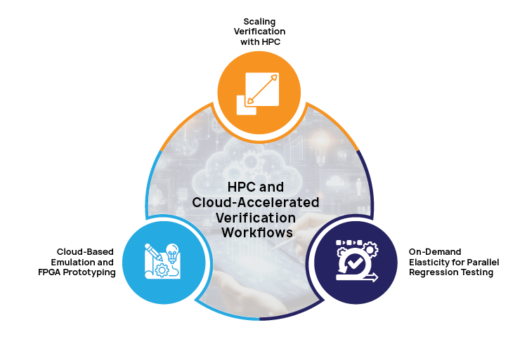
HPC and Cloud-Accelerated Verification Workflows
The verification phase in semiconductor design demands immense computational power to validate complex architectures, ensure functional correctness, and optimize manufacturability. Traditional on-premise verification environments struggle to keep pace with the increasing volume of regression tests, formal verification cycles, and deep learning-driven test generation. High-performance computing (HPC) and cloud-based acceleration are redefining verification workflows by offering scalable, on-demand computing resources.
- Scaling Verification with HPC: Cloud-integrated HPC platforms dynamically allocate compute resources to handle large-scale verification workloads, including formal verification, functional verification, and Design-for-Test (DFT) processes. This scalability reduces verification turnaround time and enhances test coverage without infrastructure limitations.
- On-Demand Elasticity for Parallel Regression Testing: Cloud-based verification environments enable running thousands of regression tests in parallel, leveraging distributed computing clusters. By eliminating hardware bottlenecks, engineers can execute exhaustive validation scenarios simultaneously, ensuring higher test efficiency and faster design signoff.
- Cloud-Based Emulation and FPGA Prototyping: Pre-silicon validation is accelerated through cloud-driven emulation and FPGA prototyping. Cloud-hosted hardware emulation platforms enable real-time validation of complex SoC architectures, while FPGA-based prototyping allows early firmware and software testing, reducing post-silicon debugging efforts.
Cloud Integration in Tape-Out and Foundry Collaboration
As semiconductor designs reach tape-out, cloud-based EDA ensures seamless integration with leading foundries, streamlining Design for Manufacturability (DFM) validation and secure data transmission. By eliminating traditional bottlenecks in final design handoff, cloud-enabled workflows enhance efficiency, accuracy, and security in the critical last mile of chip production.
- Direct Foundry Integration: Cloud-native EDA platforms connect directly with major foundries, enabling real-time collaboration for DFM checks, lithography simulations, and process rule compliance before fabrication. This ensures that designs meet manufacturing constraints without last-minute modifications.
- Cloud-to-Foundry DFM Validation: Advanced DFM engines leverage cloud computing to analyze full-chip layouts at scale, running complex lithography, etching, and chemical-mechanical polishing (CMP) simulations. Cloud-powered DFM reduces design iterations by detecting and rectifying potential yield issues early.
- Secure Data Transmission for Tape-Out: Cloud-native foundry interfaces facilitate encrypted and access-controlled transfers of GDSII and OpenAccess databases, ensuring the integrity and confidentiality of final design data. Role-based encryption and blockchain-enabled audit trails further enhance IP protection during the handoff process.
Challenges in Cloud-Based EDA Adoption and Future Directions
While cloud-based Electronic Design Automation (EDA) offers scalability, parallelism, and AI-driven optimizations, its adoption presents several challenges that semiconductor design teams must overcome. Addressing these technical constraints is crucial to unlocking the full potential of cloud-powered chip design.
- Overcoming Latency and Data Transfer Bottlenecks: Cloud-hosted EDA workflows require rapid data transfer between local design environments and remote cloud servers. High-latency connections can disrupt synthesis, place-and-route, and verification processes, impacting design turnaround time. Implementing edge computing for pre-processing, leveraging high-bandwidth cloud interconnects, and optimizing data compression techniques can mitigate these challenges.
- Managing Cloud Costs and Optimizing Resource Utilization: Unlike fixed on-premise infrastructure, cloud-based EDA follows a pay-as-you-go model, making cost management critical. Inefficient workload distribution, redundant simulations, and underutilized compute resources can escalate expenses. AI-powered workload orchestration, predictive scaling, and dynamic resource allocation help optimize costs while maintaining performance.
- Future of Quantum Computing in Cloud-Based Semiconductor Design: As semiconductor scaling nears physical limits, quantum computing emerges as a potential disruptor in cloud-EDA workflows. Quantum algorithms can revolutionize combinatorial optimization problems in place-and-route, lithography modeling, and material simulations. Cloud-accessible quantum processors, coupled with classical EDA tools, may redefine next-generation chip design paradigms.
Conclusion
The future of silicon engineering is undeniably cloud-driven, with cloud-based EDA playing a pivotal role in accelerating next-generation semiconductor innovation. As chip complexity increases and design cycles shrink, adopting cloud-integrated EDA workflows is no longer optional—essential for maintaining a competitive edge. By leveraging scalable computing resources, seamless collaboration, and AI-powered automation, semiconductor companies can optimize design efficiency, reduce costs, and accelerate time-to-market.
At ACL Digital, we bring deep expertise in silicon engineering, helping our customers navigate this transformation through tailored cloud-enabled solutions. Our proven experience in semiconductor design, verification, and validation, coupled with strong collaborations with industry leaders, empowers companies to embrace cloud-first methodologies and drive innovation at scale. As the semiconductor landscape evolves, ACL Digital remains committed to delivering cutting-edge engineering solutions that redefine the future of chip design.
Connect with our experts to know more in detail.
Related Insights

Securing Agentic AI-Based Systems
Vinayak Sakhare


Zero-Trust AI: Securing MCP-Based LLM Systems in Production
Siddharth Dange