TSMC North America 2025 Open Innovation Platform Ecosystem Forum
The 2025 TSMC Open Innovation Platform Ecosystem Forum, held at the Santa Clara Convention Center, brought together industry leaders and innovators to explore the future of semiconductor design and innovation. At our booth, visitors had the opportunity to learn about the latest advancements in AI chips, with a special focus on AI accelerators built on TSMC’s N6-to-N2 nodes, HBM-integrated designs, PCIe/UCIe subsystem architectures, and cutting-edge custom analog IP products.
As a TSMC Open Innovative Platform® (OIP) DCA partner, ACL Digital showcased the latest advancements in SoC, ASIC, and embedded software, including end-to-end AI chip design, HBM, and UCIe-enabled accelerator integrations, as well as expertise in node migration. We highlighted how we drove innovation in AI and silicon technology.
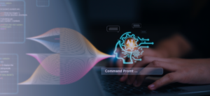
At ACL Digital, we go beyond engineering to empower the next wave of digital transformation at the intersection of AI/ML, HPC, SERDES IP design, and IP porting. We specialize in AI accelerators and subsystem integration (PCIe, UCIe, HBM), and design for Functional Safety (FuSa/ISO 26262) across advanced nodes. Through our specialized Centers of Excellence, we support businesses to drive progress in automotive semiconductors, IoT, 5G, wireless networking, and semiconductor global capability centers.
Centres of Excellence & Trusted Semiconductor Collaborations
TSMC Design Centre Alliance
RISC-V Centre of Excellence
ARM Approved Design Partner
Functional Safety & ISO 26262 Centre of Excellence
Core Strengths
RTL to GDS II
PCIe/UCIe/ETHERNET/DDR Sub Systems
Physical implementation for leading-edge TSMC nodes